
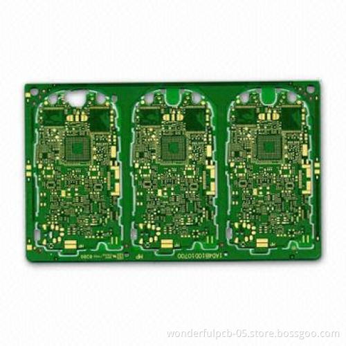
4-layered Electronic Circuit PCB with FR4 Material, HASL Finish, Blind, Buired Vias for LED, Assembl
- Payment Type:
- Telegraphic Transfer in Advance (Advance TT, T/T)
Your message must be between 20 to 2000 characters
Contact Now| Payment Type: | Telegraphic Transfer in Advance (Advance TT, T/T) |
|---|
- Layers: 1 to 28
- Board finished thickness: 0.2 to 7.0mm
- Materials: FR-4, CEM-1, CEM-3, high TG, FR4 halogen free andRogers
- Finished board size: 23 x 25 (580 x 900mm) (maximum)
- Drilled hole size: 3 mils (0.075mm) (minimum)
- Line width: 3 mils (0.075mm) (minimum)
- Line spacing: 3 mils (0.075mm) (minimum)
- Surface finish/treatment: HASL/HASL lead free, HAL, chemicaltin and chemical gold, immersion silver/gold, OSP and goldplating
- Copper thickness: 0.5 to 7.0oz
- Solder mask colors: green/yellow/black/white/red/blue
- Copper thickness in hole: >25.0μm (>1-mil)
- Inner packing: vacuum packing/plastic bag
- Outer packing: standard carton packing
- Shape tolerance: ±0.13
- Hole tolerance:
- PTH: ±0.076
- NPTH: ±0.05
- Certificates: UL-SGS-RoHS-approved
- Special requirements: buried and blind vias + controlledimpedance + BGA
- Profiling: punching, routing, V-cut and beveling
- Provides OEM services to all sorts of printed circuit boardassembly as well as electronic encased products
- PTH: ±0.076
- NPTH: ±0.05
-

Mobile HDI PCB with 0.5 to 7.0oz Copper Thickness and 1 to 28 Layers
-
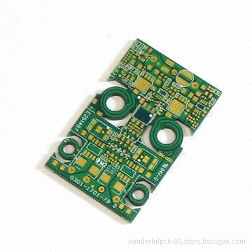
Electronic Circuit, Widely Used for Customer Electronics, Punching, and Routing Profiling
-

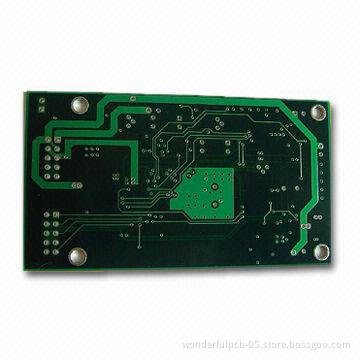
High Quality Multilayer PCB with 4mil Line Width and 0.3mm Minimum Hole Size
-

High-density Multilayer PCB with 0.21 to 7.0mm Board Finished Thickness
Related Keywords
-
Mobile HDI PCB with 0.5 to 7.0oz Copper Thickness and 1 to 28 Layers
Electronic Circuit, Widely Used for Customer Electronics, Punching, and Routing Profiling
High Quality Multilayer PCB with 4mil Line Width and 0.3mm Minimum Hole Size
High-density Multilayer PCB with 0.21 to 7.0mm Board Finished Thickness

Four-layer FPC with ENIG Surface Finish and PI 0.2mm Thickness
Related Products-
High-density Multilayer PCB with 0.21 to 7.0mm Board Finished Thickness
-
Mobile HDI PCB with 0.5 to 7.0oz Copper Thickness and 1 to 28 Layers
-

HDI Board with 8 Layers and Immersion Gold Surface Technique
-

PCB Board for Industrial Use, with FR-4 Base Material
-
PCBA for CCTV Field, with 580 x 900mm Maximum Finished Board Size
Product Categories-
Multilayer PCBs(114)
-
Double-sided PCBs(89)
-
PCB assemblies(85)
-
High-density multilayer PCBs(68)
-
Aluminum PCBs(62)
-
Flexible PCBs(63)
-
Single-sided PCBs(43)
-
Rigid-flex PCBs(25)
-
Single-sided flexible PCBs(20)
-
Multilayer flexible PCBs(15)
-
Quick-turnaround PCBs(14)
-
PCB laminates(15)
-
PCB design services(10)
-
Split flexible PCBs(9)
-
Double-sided flexible PCBs(6)
-
Double access flexible PCBs(6)
-
Laptop motherboards(5)
-
Immersion gold PCBs(5)
-
Lead free HAL PCBs(5)
-
PCB connectors(3)
-
Immersion silver PCBs(3)
-
Contract manufacturing services(3)
-
PCB terminal blocks(1)