

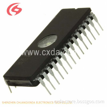
M27C256B-45F6
- Payment Type:
- L/C, T/T, Western Union, MoneyGram
- Delivery Time:
- 1 Days
Quantity:
Your message must be between 20 to 2000 characters
Contact NowBasic Info
Basic Info
| Place of Origin: | Malaysia |
|---|---|
| Supply Ability: | 30000 Piece/Pieces per Week |
| Payment Type: | L/C,T/T,Western Union,MoneyGram |
Product Description
Product Description
Specifications >M27C256B 256 Kbit (32b x 8)UV EPROM
>Brand:ST
>D/C:10+ original
>Best price,Reliable quality parts,Ontimes delivery
Feature summary
5V ± 10% SUPPLY VOLTAGE in READ
OPERATION
ACCESS TIME: 45ns
LOW POWER CONSUMPTION:
– Active Current 35mA at 5MHz
– Standby Current 100μA
PROGRAMMING VOLTAGE: 12.75V ± 0.25V
PROGRAMMING TIME: 50μs/word
ELECTRONIC SIGNATURE
– Manufacturer Code: 20h
– Device Code: 42h Summary description
The M27C256B is a 256 Kbit EPROM offered in the two ranges UV (ultra violet erase) and OTP (one time programmable). It is ideally suited for microprocessor systems and is organized as 32,768 by 8 bits.Device operation
The operating modes of the M27C256 are listed in the Operating Modes table. A single
power supply is required in the read mode. All inputs are TTL levels except for VPP and 12V
on A9 for Electronic Signature. Programming
When delivered (and after each erasure for UV EPROM), all bits of the M27C256 are in the
'1' state. Data is introduced by selectively programming '0's into the desired bit locations.
Although only '0's will be programmed, both '1's and '0's can be present in the data word.
The only way to change a '0' to a '1' is by die exposure to ultraviolet light (UV EPROM). The
M27C801 is in the programming mode when VPP input is at 12.75V, G is at VIH and E is
pulsed to VIL. The data to be programmed is applied to 8 bits in parallel to the data output
pins. The levels required for the address and data inputs are TTL. VCC is specified to be
6.25V ± 0.25V. Maximum rating
Stressing the device above the rating listed in the Absolute Maximum Ratings table may
cause permanent damage to the device. These are stress ratings only and operation of the
device at these or any other conditions above those indicated in the Operating sections of
this specification is not implied. Exposure to Absolute Maximum Rating conditions for
extended periods may affect device reliability. Refer also to the STMicroelectronics SURE
Program and other relevant quality documents. ....
>Brand:ST
>D/C:10+ original
>Best price,Reliable quality parts,Ontimes delivery
| Datasheets | M27C256B |
|---|---|
| Product Photos | M27C256B-45F6 |
| Standard Package | 13 |
| Category | Integrated Circuits (ICs) |
| Family | Memory |
| Series | - |
| Format - Memory | EPROMs |
| Memory Type | UV EPROM |
| Memory Size | 256K (32K x 8) |
| Speed | 45ns |
| Interface | Parallel |
| Voltage - Supply | 4.5 V ~ 5.5 V |
| Operating Temperature | -40°C ~ 85°C |
| Package / Case | 28-CDIP (0.600", 15.24mm) Window |
| Packaging | Tube |
| Supplier Device Package | 28-CDIP Frit Seal with Window |
| Catalog Page | 964 (CN081 PDF) |
5V ± 10% SUPPLY VOLTAGE in READ
OPERATION
ACCESS TIME: 45ns
LOW POWER CONSUMPTION:
– Active Current 35mA at 5MHz
– Standby Current 100μA
PROGRAMMING VOLTAGE: 12.75V ± 0.25V
PROGRAMMING TIME: 50μs/word
ELECTRONIC SIGNATURE
– Manufacturer Code: 20h
– Device Code: 42h Summary description
The M27C256B is a 256 Kbit EPROM offered in the two ranges UV (ultra violet erase) and OTP (one time programmable). It is ideally suited for microprocessor systems and is organized as 32,768 by 8 bits.Device operation
The operating modes of the M27C256 are listed in the Operating Modes table. A single
power supply is required in the read mode. All inputs are TTL levels except for VPP and 12V
on A9 for Electronic Signature. Programming
When delivered (and after each erasure for UV EPROM), all bits of the M27C256 are in the
'1' state. Data is introduced by selectively programming '0's into the desired bit locations.
Although only '0's will be programmed, both '1's and '0's can be present in the data word.
The only way to change a '0' to a '1' is by die exposure to ultraviolet light (UV EPROM). The
M27C801 is in the programming mode when VPP input is at 12.75V, G is at VIH and E is
pulsed to VIL. The data to be programmed is applied to 8 bits in parallel to the data output
pins. The levels required for the address and data inputs are TTL. VCC is specified to be
6.25V ± 0.25V. Maximum rating
Stressing the device above the rating listed in the Absolute Maximum Ratings table may
cause permanent damage to the device. These are stress ratings only and operation of the
device at these or any other conditions above those indicated in the Operating sections of
this specification is not implied. Exposure to Absolute Maximum Rating conditions for
extended periods may affect device reliability. Refer also to the STMicroelectronics SURE
Program and other relevant quality documents. ....


Related Keywords
Related Keywords
You May Also Like
You May Also Like

