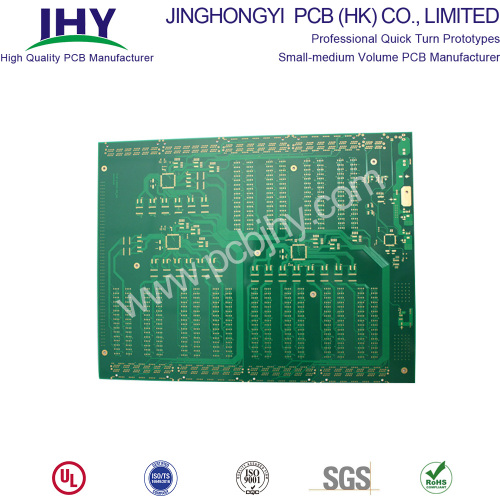


4 Layer Prototype Multilayer PCB Stackup and Manufacturing
- Payment Type:
- L/C, T/T, D/P, Paypal, Money Gram, Western Union
- Incoterm:
- FOB, CFR, CIF, EXW, FCA, CPT, CIP
- Min. Order:
- 1 Piece/Pieces
- Min. Order:
- 1 Piece/Pieces
- Transportation:
- Ocean, Air
Your message must be between 20 to 2000 characters
Contact Now| Place of Origin: | China |
|---|---|
| Productivity: | 10000 |
| Payment Type: | L/C,T/T,D/P,Paypal,Money Gram,Western Union |
| Incoterm: | FOB,CFR,CIF,EXW,FCA,CPT,CIP |
| Certificate: | ISO9001 |
| Transportation: | Ocean,Air |
4 Layer Prototype Multilayer PCB More layers it is, more complex & difficult the manufacturing will be, and more expensive the cost will be. The lead time of multi-layer PCB is different from normal one, please contact us for a exact lead time.
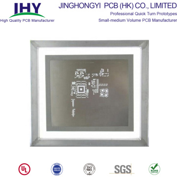
Structure of Multi-Layer PCB
- Top silkscreen/Legend: to identify name of each PAD, board part number, data, etc;
- Top Surface finishing: to protect exposed copper from oxidation ;
- Top Soldermask (overlay): to protect the copper from oxidation, to be not soldered during SMT process;
- Top Trace: copper etched according to design to carry on different function
- Substrate/Core material: Non-conductive such as FR4, FR5
- Prepreg (PP)
- Middle Layers, such as GND, VCC, Inner 3, Inner 4, etc.
- Prepreg (PP)
- Bottom trace (if any): (same as above mentioned)
- Bottom soldermask (overlay):(same as above mentioned)
- Bottom surface finishing: (same as above mentioned)
- Bottom silkscreen/legend: (same as above mentioned)
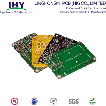
Product & Service
- Quick Turn PCB
- Rigid PCB
- Flexible PCB
- Rigid-flex PCB
- Aluminum PCB
- PCB Stencil
- Multilayer PCB
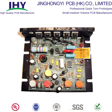
4 Layer Prototype Multilayer PCB Factory


Why choose us?
- Save money&time! Achieve peace of mind!
- A professional and trustworthy PCB prototype manufacturer.
- Fastest PCB Prototype.
- One stop solution for various PCB&SMT Stencil.
- Low cost for simple PCB.
- Affordable price for high-tech PCB.
- Minimum orders 1pcs.
- 24-hour online customer service.
- Professional PCB engineer for one-to-one service.
- Shipment on time.
-
Guarantee good service and quality from PCB quotation to delivery.
Certification(UL:E466618, TS16949, ISO9001.RoHS)
 |
 |
 |
PCB Shipment
JHY PCB offers flexible shipping methods for our customers, you may choose from one of the methods below.

Shipping Process
After production and testing, your PCB orders will be sent to our shipping department. As the quick turn PCB manufacturer, JHY PCB shipping department will ship your PCB quickly without any pending.
JHY PCB 's Packing Way
- Use one professional PCB vacuum bag, with desiccant inside. Vacuum compressed totally.
- Paste label and RoHs mark. Use second vacuum bag to protect boards again, vacuum compressed, make sure no exception.
- Microsection report and Tin testing board are put together with PCB in cartons.COC (Certificate of Conformity) will be sent to customer by email in PDF.
- Several layers of thick EPE(Expand aple poly ephylene) are filled fully in gaps between PCBs and cartons. Thickness of 1 layer EPE is 10mm.
- Neutral Packing is adopted if no special requirements. Strong and thick cartons(Thickness:10mm,7 layers). Different sizes of cartons are designed to meet demand of different PCB size. All package are within weight limit of cartons. For mass production order, no exceed 21kg per carton normally.
- All cartons sealed with strong adhesive tape should be sealed twice so as to make them more durable.
- Solid PP/PET strapping is used outside of cartons.
- Shipping mark, fragile mark and postcode label are all pasted clearly.
How to ship your PCB?
- Firstly, JHY PCB shipping department will print order address and invoice.
- Secondly, JHY PCB will set the shipment information on the Logistics company website.
- Thirdly, the Logistics company staff will collect the package from JHY PCB and ship it to you.
Shipment Term
With the purpose of better customer service and meeting the customer demand, JHY PCB provides following shipping methods.
JHY PCB is experienced in exporting. For PCB Prototype and small-medium volume PCB order, we have stable and long-term good relationship with forwarder, such as international express company DHL, FedEx, TNT, UPS. For mass production order, we have famous and reliable shipping company for support.
FAQ
Q1:What is your minimum order quantity?
A:Our MOQ is 1 PCS.
Q2: Do you accept PCB design with different boards on one panel?
A: Of course, we can do different boards on the same panel.
Q3. Are my Gerber Files safe?
A: We protect the intellectual property for customers in the whole process. All documents from customers are never shared with any third parties.
Q4:What is needed for quotation?
A:Quantity, PCB Gerber file, Technical requirements(material, board thickness ,surface finish, copper thickness,solder mask color, silkscreen color ,...)
Q5.How to quote shipping cost?
A: The shipping cost is determined by the shipment way(forwarder name,delievery days),destination, weight&dimension of packages. If you use your own forwarder ,please inform us.

Related Keywords
-
PCB Assembly SMT PCB Stencil PCB Stencil Maker
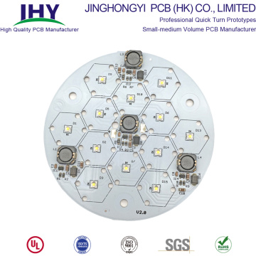
High Quality 24V LED PCB Circuit Board Assembly
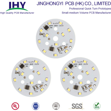
Customized Single-sided 12V SMD LED PCB Circuit Board
Related ProductsProduct Categories-
PCB Prototype(97)
-
Quick Turn PCB(33)
-
LED PCB(114)
-
Single Sided PCB(15)
-
Double Sided PCB(60)
-
Multilayer PCB(149)
-
Rigid PCB(22)
-
Flexible PCB(48)
-
Rigid Flex PCB(43)
-
Aluminum PCB(62)
-
Metal Core PCB(50)
-
Thick Copper PCB(106)
-
HDI PCB(61)
-
Impedance Control PCB(27)
-
BGA PCB(11)
-
High TG PCB(32)
-
Fr4 PCB(44)
-
Gold Fingers PCB(29)
-
PCB Application(5)
-
PCB Stencil(56)
-
PCB Assembly Service(67)
-
High Frequency PCB(47)