

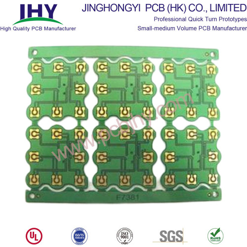
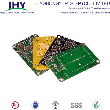
Immersion Gold Single Sided PCB Board
- Payment Type:
- L/C, T/T, D/P, Paypal, Money Gram, Western Union
- Incoterm:
- FOB, CFR, CIF, EXW, FCA, CPT, CIP
- Min. Order:
- 1 Piece/Pieces
- Min. Order:
- 1 Piece/Pieces
- Transportation:
- Ocean, Air
Your message must be between 20 to 2000 characters
Contact Now| Place of Origin: | China |
|---|---|
| Productivity: | 10000 |
| Payment Type: | L/C,T/T,D/P,Paypal,Money Gram,Western Union |
| Incoterm: | FOB,CFR,CIF,EXW,FCA,CPT,CIP |
| Certificate: | ISO9001 |
| Transportation: | Ocean,Air |
Keywords:Single Side Immersion Gold PCB, Single Side Plating PCB, Manufacturing Process of Single Sided PCB
Immersion Gold is a kind of PCB surface treatment process. Other processes include: Immersion Tin, Immersion Silver, HASL, lead-free HASL, ENIG, Flash gold, Thick gold, Selective gold plating, OSP, Selective OSP /HASL, etc.
The purpose of immersion gold process is to deposit nickel gold coating on the surface of the printed circuit board (such as single-sided printed circuit board, double-sided PCB, multilayer PCB, rigid PCB, etc.) with stable color, good brightness, flat coating, and good weldability. It can be basically divided into four stages: pre-treatment (degreasing, micro etching, activation, post leaching), nickel deposition, gold deposition, post-treatment (waste gold washing, di washing, drying).
The thickness of immersion gold is 0.025-0.1um.
The immersion gold is a chemical deposition. A layer of coating is formed by a chemical oxidation-reduction reaction. Generally, the thickness is relatively thick. It is one of the deposition methods of the chemical nickel gold layer, which can achieve a relatively thick gold layer.
In the practical application of products, 90% of them are immersion gold board, because the poor weldability of plating gold plate is his fatal defect, and it is also the direct reason for many companies to give up the gold plating process!
Gold is used for surface treatment of circuit board because of its strong conductivity, oxidation resistance and long service life. General applications such as button PCB, gold finger PCB, etc., and the most fundamental difference between gold-plated PCB and immersion gold PCB is that gold plating is hard gold (wear-resistant), and immersion gold is soft gold (non wear-resistant).
Why to use immersion gold PCB
The immersion gold PCB mainly has the following characteristics:
1. The crystal structure of immersion gold is different from that of gold plating. The thickness of immersion gold is much thicker than that of gold plating. The immersion gold will be golden yellow, more yellow than that of gold plating (this is one of the methods to distinguish gold plating from immersion gold), and the gold plating will be slightly white (nickel color).
2. The crystal structure of immersion gold is different from that of gold plating. Compared with gold plating, immersion gold is easier to weld and will not cause poor welding. The stress of the sinking plate is easier to control, which is more conducive to the processing of the bonded products. At the same time, it is because the immersion goldis softer than the gold plate, so the gold finger made of the immersion goldis not wear-resistant (the disadvantage of the immersion gold).
3. There is only nickel gold on the solder pad of the immersion gold PCB board, and the signal transmission in the skin effect is that the copper layer will not affect the signal.
4. The crystal structure of immersion gold is more compact than that of gold plating, which is not easy to produce oxidation.
5. With the increasing requirements for the processing accuracy of the circuit board, the line width and spacing have reached below 0.1mm. Gold plating is easy to produce short circuit. Only the pad of the immersion gold board has nickel gold, so it is not easy to produce a short circuit of gold wire.
6. Only the pad of the immersion gold plate has nickel gold, so the combination of the resistance welding and the copper layer on the line is stronger. The project will not affect the spacing when making compensation.
7. For the boards with high requirements, the flatness is required to be good. Generally, the immersion gold is used, and the phenomenon of the black pad after assembly will not appear. The flatness and service life of the immersion gold is better than that of the gold plate.
Why choose us?
With Nearly 10 years of PCB manufacturing experience, JingHongYi PCB (HK) Co., Limited is rapidly becoming the logical choice for PCB manufacturers in Shenzhen, China. We're proud to manufacture high-quality products. We can handle production orders on 1 layers all the up to 24 layers(single sided PCB, double sided PCB, multilayer PCB, rigid PCB, flexible PCB, high-frequency PCB, etc.). and we have quick turn , Small volume and large volume service type PCB assembly services without MOQ.
No MOQ, low cost for small quantity prototype. We penalize prototype circuit boards on a big panel which will share set-up costs with other customers, which could save a lot of PCB tooling cost for small quantity PCB prototype. PCB manufacturing on spec. We have professional engineering in each production process from evaluating cost, checking and assessing Gerber requirement, making MI to production and final inspection to guarantee circuit board quality. Meeting your printed circuit board needs from PCB prototyping to mid-volume production ISO/TS certified PCB manufacturing factory. Deliver on time. We keep higher than 99% on-time-delivery rate Combined service to arrange your PCB to you by DDU TO DOOR shipment with competitive shipping cost. You don't need to arrange anything after confirming the order just wait for your PCB deliver to your hand. Offer free DRC for DFM to our customers. Decades of experience in supporting manufacturing PCB requirements from a wide range of industries.
Minimum Order Quantity: 1pcs
Price: The price will change with different process and quantity
Packaging Details: box
Delivery Time: quick turn and normal type
Payment Terms: TT, LC, and others base on negotiation
Supply Ability: 1, 000, 000PCS/week
What is Single Sided PCB
There are many similarities and differences between single sided PCB and double sided PCB, and we will also explain them here.
Single Sided PCB Manufacturing
One thin layer of thermally conductive but electrically insulating dielectric is laminated with copper. Soldermask is usually applied on top of the copper.

JHY PCB produces prototype, midrange and high volume Single Sided circuit boards, with a copper thickness from 1 to 20 ounces. Operating temperatures range from 130 C to 230 C. Single sided boards are available with surface finishes including Organic Surface Protectant (OSP), Immersion Silver, Tin, and Gold plating along with both leaded or lead-free Hot Air Solder Level (HASL).
Construction of Single Sided PCB

Above substrate, there lies a copper layer which provides conducting path for various components on the board. The copper thickness is different for different boards depending on your needs and requirements and is defined in ounces per square foot.
On the top of copper foil, there exists a solder mask layer. This layer is mainly used for protection and makes the copper foil insulating which helps in avoiding the conduction in case direct contact happens with some conducting material.
On the top of all layers, there exists a silkscreen layer that is mainly used for adding symbols and characters on the board so a common person can anticipate the clear understanding of the board.
Advantages of Single Layer PCB
- Ideal for simple low-density designs
- Lower cost, especially for high volume orders
- Lower probability of manufacturing issues
- Popular, common, and easily understood by most PCB manufacturers
Application of Single Sided PCB
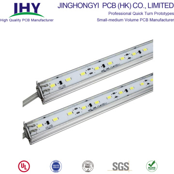
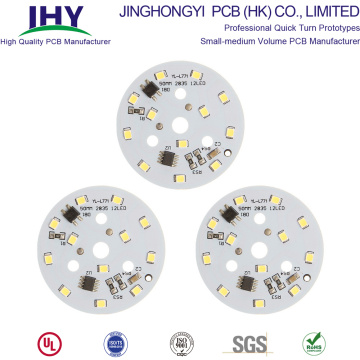
Aluminum PCB, LED PCB used in LED lighting industry are basically Single Sided PCB.
ALTHOUGH SINGLE SIDED PCBS ARE RELATIVELY SIMPLE, THEY CAN STILL BE USED IN VERY COMPLEX DEVICES:
- Power supplies
- Relays (automotive and industrial)
- Timing circuits
- Sensor products
- LED lighting
- Radio and stereo equipment
- Packaging equipment
- Surveillance
- Calculators
- Printers
- Coffee makers
- Vending machines
- Solid state drives
- Camera systems
Related Keywords
-
Metal Core Aluminum PCB Single Side PCB manufacturing
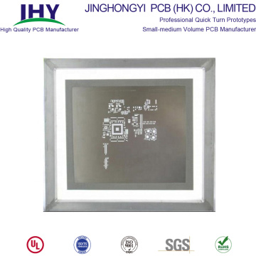
PCB Assembly SMT PCB Stencil PCB Stencil Maker
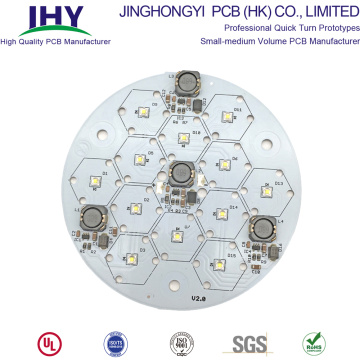
High Quality 24V LED PCB Circuit Board Assembly
Customized Single-sided 12V SMD LED PCB Circuit Board
HDI Fr4 Tg130 Tg150 Tg170 Tg180 Multilayer PCB
Related ProductsProduct Categories-
PCB Prototype(97)
-
Quick Turn PCB(33)
-
LED PCB(114)
-
Single Sided PCB(15)
-
Double Sided PCB(60)
-
Multilayer PCB(149)
-
Rigid PCB(22)
-
Flexible PCB(48)
-
Rigid Flex PCB(43)
-
Aluminum PCB(62)
-
Metal Core PCB(50)
-
Thick Copper PCB(106)
-
HDI PCB(61)
-
Impedance Control PCB(27)
-
BGA PCB(11)
-
High TG PCB(32)
-
Fr4 PCB(44)
-
Gold Fingers PCB(29)
-
PCB Application(5)
-
PCB Stencil(56)
-
PCB Assembly Service(67)
-
High Frequency PCB(47)


