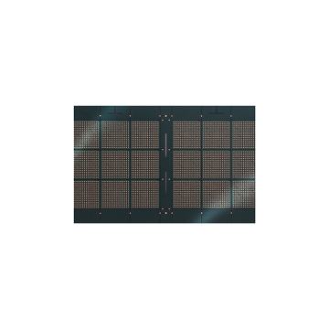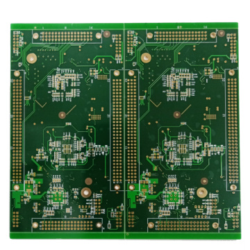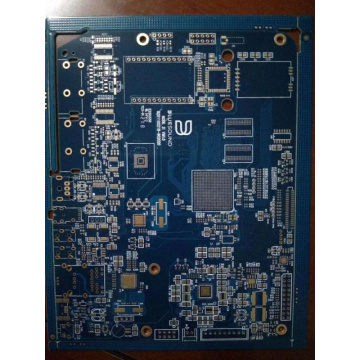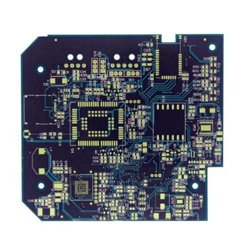
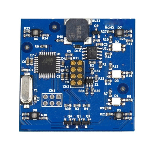
Fiber Switch Pcba 2 layer Pcb Assemble
-
$0.02≥1 Piece/Pieces
- Min. Order:
- 1 Piece/Pieces
- Min. Order:
- 1 Piece/Pieces
Your message must be between 20 to 2000 characters
Contact NowHow do you make a two layer PCB?
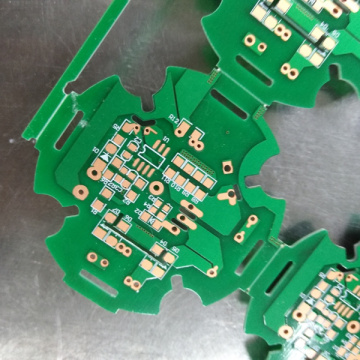
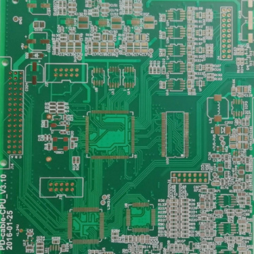
Custom pcb fabrication is the carrier of electronic design. It is the place where all electronic components and circuits are summarized. Nowadays, electronic products have more and more functions, more and more components are included, and circuit designs are becoming more and more complex. The most basic Single-sided boards are no longer universal. When single-sided circuits are not enough to provide electronic parts connection requirements, the circuits can be arranged on both sides of the substrate, and through-hole circuits can be deployed on the board to connect the circuits on both sides of the board. This type of pcb board is called a double-layer pcb board.
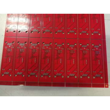
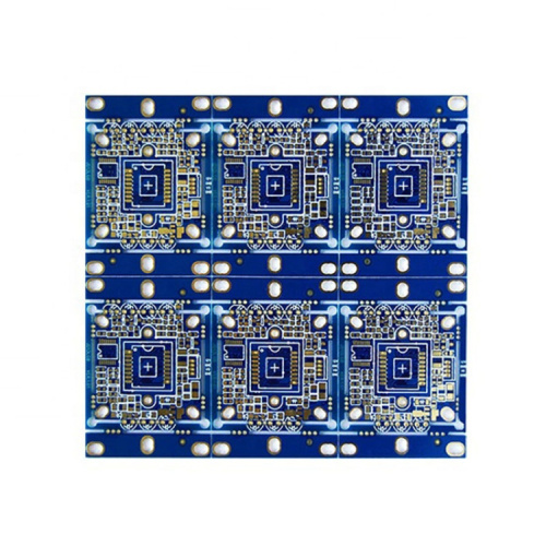
Double-layer PCB board production process and technology:
The production process of double-layer PCB board can be roughly divided into the following parts:
Printed circuit board-inner circuit-pressing-drilling-plated through hole (primary copper)-outer circuit (secondary copper)-solder resist green paint-text printing-contact processing-forming cutting-final inspection packaging.


Related Keywords