
fast and efficient PCB design and custom PCB
-
$8.00≥8 Piece/Pieces
- Min. Order:
- 8 Piece/Pieces
- Min. Order:
- 8 Piece/Pieces
- Transportation:
- Ocean, Land, Air, Express, Others
Quantity:
Your message must be between 20 to 2000 characters
Contact NowBasic Info
Basic Info
| Payment Type: | T/T,Paypal,Others |
|---|---|
| Incoterm: | EXW,FOB |
| Transportation: | Ocean,Land,Air,Express,Others |
Product Description
Product Description
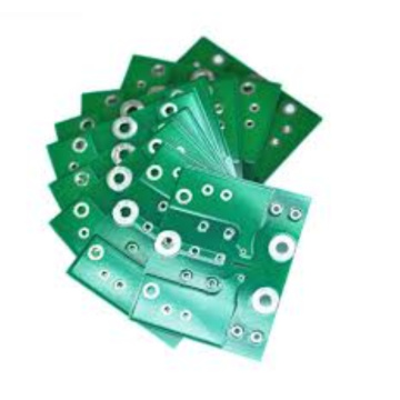
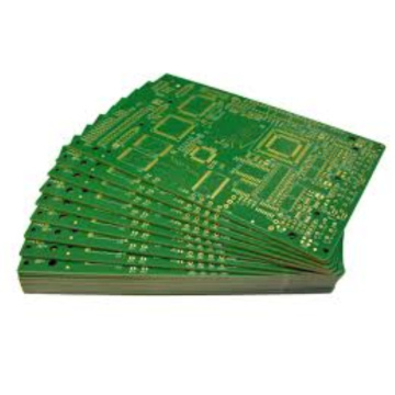
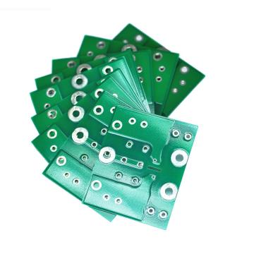
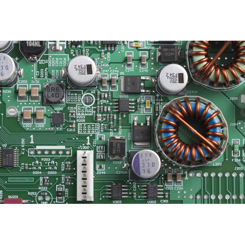
Many PCB circuit board production enthusiasts often like to make some circuit boards by themselves in their spare time.
Production method one:
1. Cut the copper-clad board to the size required by the circuit diagram.
2. Put the wax paper on the steel plate, use a pen to engrave the circuit diagram on the wax paper 1:1, and cut the circuit diagram engraved on the wax paper according to the size of the circuit board, and place the cut wax paper on the printed copper board. Take a small amount of paint and talcum powder to make a suitable thin and thick printing material, dip the printing material with a brush, and evenly apply it to wax paper, repeat it several times, and the circuit can be printed on the printed board. This kind of stereotype can be used repeatedly and is suitable for small batch production.
3. Use 1 gram of potassium chlorate and 40 milliliters of 15% hydrochloric acid to prepare a corrosive solution, and apply it to the corroded area on the circuit board for corrosion.
4. Wash the corroded printed board with water repeatedly. Wipe off the paint with banana water, and then wash it several times to make the printed board clean without leaving corrosive liquid. Apply a layer of rosin solution and let it dry before drilling holes.
Production method five:
1. Reasonably arrange the density of the components and the position of each component according to the shape of the components used in the circuit schematic and the size of the printed board area. The location of the components should be determined according to the principle of large first, then small, first overall and then local, so that adjacent components in the circuit are placed nearby and arranged neatly and evenly.
2. The connecting wires between the components cannot be turned at right angles at the corners and the intersection of the two lines, they must be transitioned by curves, and they must not cross each other and turn too far. When some wires can't do this, you can consider printing wires on the reverse side of the printed board, and then use studs to connect with the front circuit, or use insulated wires when soldering components.
3. It is better for the input part and the output part to be farther apart to avoid mutual interference.


Related Keywords
Related Keywords
You May Also Like
You May Also Like