What are the steps involved in manufacturing a flexible PCB?
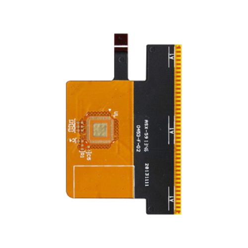
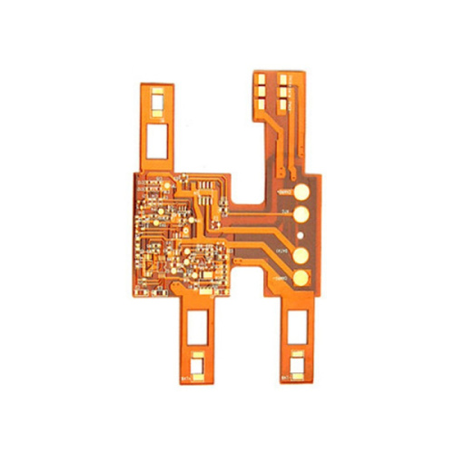
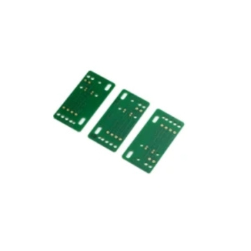
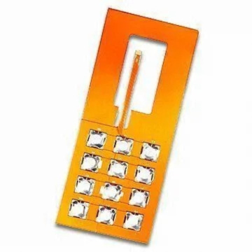
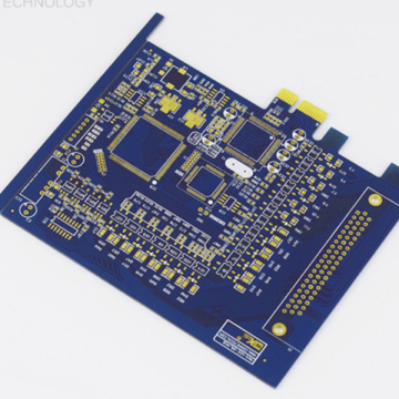
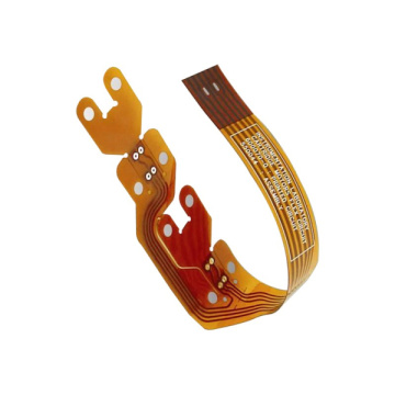
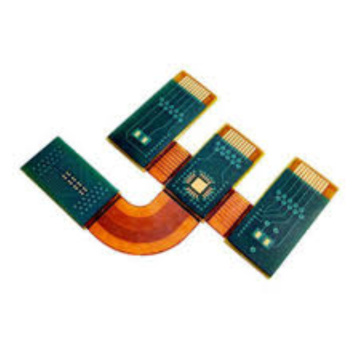
The flexible circuit board (flexibleprintcircuit; fpc) is made by bonding a flexible copper foil substrate (fccl) and a flexible insulating layer with an adhesive (adhesive), and then undergoing etching and other processing processes, and finally leaving the required conductive traces Wire, as a medium for the transmission of electricity or electronic signals. Flexible circuit boards can be used in a wide range of fields including computers and peripherals, communication products, consumer electronics, automobiles, and military, among which communication products account for the most important proportion. The materials used in the flexible insulating layer of the flexible circuit board can be divided into polyimide film (pifilm) and polyester resin film (petfilm). Among them, pi film (pifilm) is most commonly used.
The structure of flexible circuit boards can be divided into two-layer structure of non-adhesive soft board (2layerfccl) and three-layer structure of glueless soft board (3layerfccl). The biggest difference between the two is the difference between copper foil and polyimide film. Whether there is an adhesive in between. Since the three-layer structure of the flexible substrate with adhesive has an adhesive, it can only tolerate a short heat treatment time, and its reliability will be reduced due to the deterioration of the adhesive caused by the heat treatment. The adhesive will also have film stress, copper atom migration and Various problems with electroplating solution penetration. In contrast, the two-layer structure of the non-adhesive flexible substrate does not have the above-mentioned problems of the three-layer structure of the adhesive-free flexible substrate.
At present, the main manufacturing methods of the two-layer structured non-adhesive flexible board include: casting, lamination, sputtering/plating, and electrolessplating. The coating method is to coat pi varnish on a thin copper foil and then heat to over 300°C for polyimide condensation (polyimidecondensation) to form a two-layer structure of non-adhesive soft board substrate. The coating method can be Obtain good bonding strength between pi film and copper foil. The pressing method is formed by pressing the thermoplastic pi film and copper foil under high temperature and high pressure, and the custom circuit board cost manufacturing is relatively high. The sputtering/electroplating method is a method of directly depositing copper on the pi film, in which the adhesion between the deposited copper and the pi film is the smallest among the above three methods. Electroless copper plating is a technique known in the field of printed circuit board (pcb) manufacturing. It is known that electroless copper plating is used to form a conductive circuit on the surface of a non-metallic substrate of a printed circuit board. First, a catalyst is also called The catalyst performs the surface treatment of the substrate to adsorb a layer of active particles on the surface of the non-metallic substrate. This step is generally called sensitization. The commonly used active particles for sensitization are metal palladium particles (pd ) And silver particles (ag). It is known that a catalyst containing palladium particles is an aqueous solution containing tin/palladium colloid, where the tin/palladium colloid includes a palladium metal core surrounded by a stable layer of tin ions (ii), but This catalyst has the following problems, including: poor stability of tin/palladium colloids and high price of palladium. For the manufacturing technology of the two-layer structure of the non-adhesive soft board substrate, improving the adhesion and flexibility between the pi film and the copper foil is a technical problem that needs to be overcome during the development of the manufacturing technology.
In the aforementioned known methods, nickel is used as a catalyst for copper deposition in sputtering and electroless plating processes, and the deposited copper loses adhesion properties on the film without nickel pretreatment. In the further etching process, nickel is difficult to be etched by traditional etching chemicals. In addition, the pretreatment solution is related to the treatment of the composition used. In order to better treat the used pretreatment solution, hexavalent chromium compounds and neutralized reduction products must be reduced. Hexavalent chromium is a genotoxic carcinogen and is highly dangerous. Workers exposed to hexavalent chromium are at risk of suffering from lung cancer, asthma, or damage to the nasal epithelium and skin. The use of hexavalent chromium may cause long-term pollution to the environment, and is widely banned in the electronics industry in the United States, Europe and China. While neutralizing, a large amount of chromium hydroxide is formed, and this treatment significantly hinders the removal of the composition used. In addition, the pretreatment solution of this known method is highly corrosive and requires a large amount of water to completely remove it from the surface of non-metallic materials. In addition, the conventional surface pretreatment process before electroplating is complicated and time-consuming.