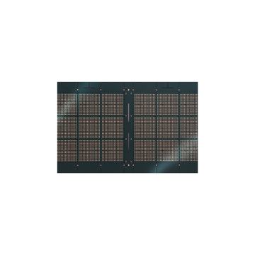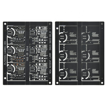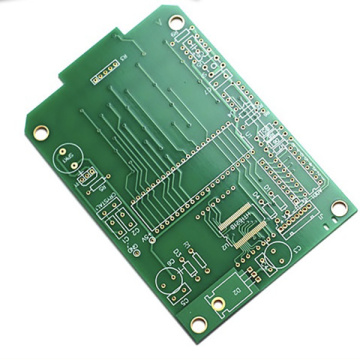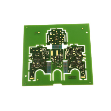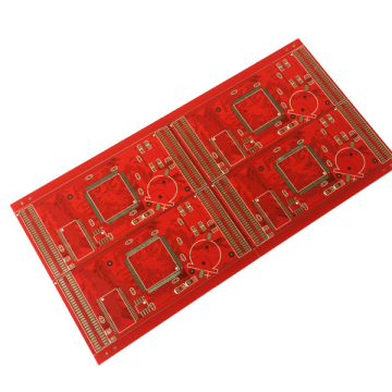


Fast Pcba Prototype Company Solder Resist Pcb
-
$10.82≥1 Piece/Pieces
- Min. Order:
- 1 Piece/Pieces
- Min. Order:
- 1 Piece/Pieces
- Transportation:
- Ocean, Land, Air, Express, Others
Your message must be between 20 to 2000 characters
Contact Now| Payment Type: | T/T,Paypal,Others |
|---|---|
| Incoterm: | FOB,EXW |
| Transportation: | Ocean,Land,Air,Express,Others |
How do you make high frequency PCB?
PCB plays an important role in fixing the circuit and optimizing the layout of electrical appliances. How about the advantages of high frequency circuit and high frequency board?
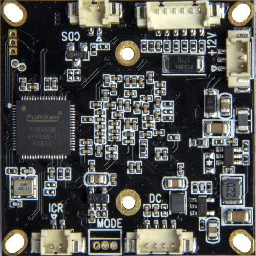
PCB is mainly composed of pads, vias, mounting holes, wires, Electronic Components, connectors, filling, electrical boundaries, etc. The main functions of each component are as follows:
Pad: A metal hole used to solder the pins of components.
Vias: There are metal vias and non-metal vias. Metal vias are used to connect component pins between layers.
Mounting hole: used to fix the circuit board.
Wire: The copper film of the electrical network used to connect the pins of the components.
Connectors: components used to connect between circuit boards.
Filling: Copper coating for ground wire network, which can effectively reduce impedance.
Electrical boundary: used to determine the size of the PCB, all Electronic Components on the PCB cannot exceed the boundary.
In the high frequency board design, the power supply is designed in the form of layers, and in most cases it is much better than the design in the form of a bus, so that the loop can always follow the path with the least impedance. In addition, the power board has to provide a signal loop for all generated and received signals on the PCB, so that the signal loop can be minimized, thereby reducing noise, which is often overlooked by low-frequency circuit designers.


Related Keywords