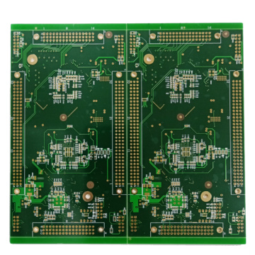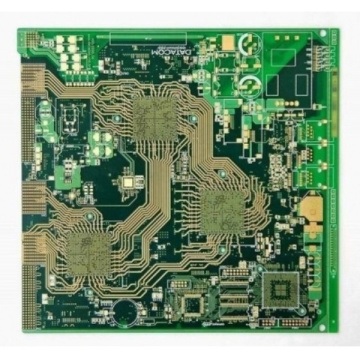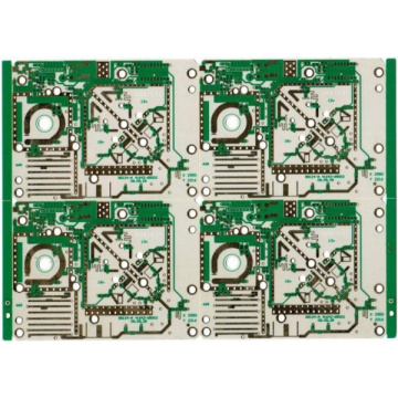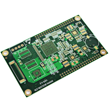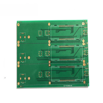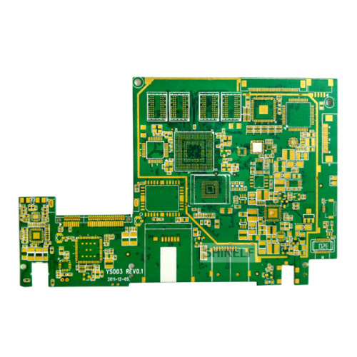
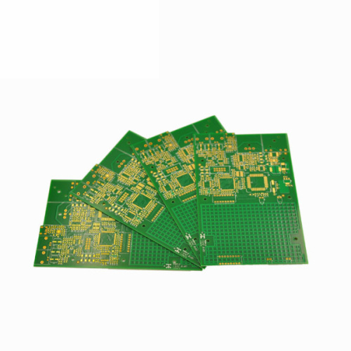
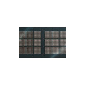
Rigid-flexible Aluminium Fr4 Double Sided Pcb Board
-
$0.10≥1 Piece/Pieces
- Min. Order:
- 1 Piece/Pieces
- Min. Order:
- 1 Piece/Pieces
Your message must be between 20 to 2000 characters
Contact NowHow is double-sided PCB made?
1. Preparation part: design the PCB, make the punching file, blank the PCB with double-sided copper-clad board, then polish the double-sided copper-clad board for CNC drilling, and check whether there are defects after polishing and drying.
2. Making vias: This is the main link. Firstly, complete the hole. After the holes are organized and standardized, they are washed and dried. After confirming that the holes are free of defects, black holes are carried out to prepare for the copper plating of the vias, and then the through holes are carried out, and then the drying is carried out ( In order to fully blacken the air, washing and drying must be performed twice). After completion, copper plating can be performed. After copper plating, polishing is performed, and the holes are checked again for defects.


The main link of double-sided PCB production
In the design of double-sided PCB boards, the layout of Electronic Components and the wiring of circuit connections are the two key links. The layout is to put the circuit components in the wiring area of the printed circuit board. Whether the layout is reasonable not only affects the subsequent wiring work, but also has an important impact on the performance of the entire circuit board. After ensuring the circuit functions and performance indicators, to meet the requirements of manufacturability, testing and maintenance, the components should be evenly, neatly and compactly placed on the PCB, and the leads and connections between the components should be minimized and shortened to obtain Uniform packing density.

When the digital circuit and the analog circuit are installed on the circuit board at the same time, the ground wire and power supply system of the two circuits are completely separated. If possible, the digital circuit and the analog circuit are arranged in different layers. When fast, medium and low-speed logic circuits need to be arranged on the circuit board, they should be placed close to the connector; and low-speed logic and memory should be placed far away from the connector. In this way, it is beneficial to reduce the reduction of common impedance coupling, radiation and crosstalk. Clock circuits and high-frequency circuits are the main sources of harassment radiation and must be arranged separately and away from sensitive circuits.


Related Keywords