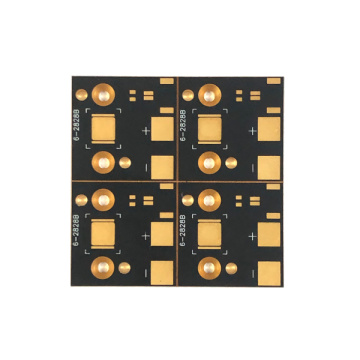
smart home automation 5g wifi module in stock
-
$1.87≥1 Piece/Pieces
- Min. Order:
- 1 Piece/Pieces
- Min. Order:
- 1 Piece/Pieces
Your message must be between 20 to 2000 characters
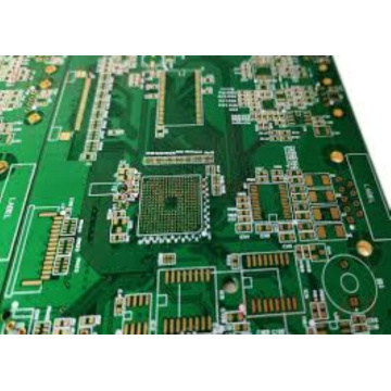
Contact NowHow PCB is assembled?
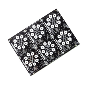
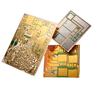
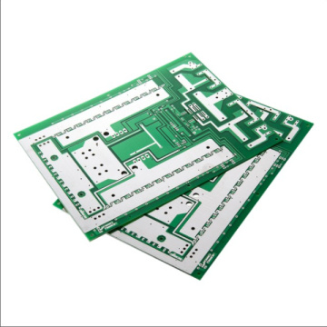
In the component interconnection technology of electronic products, the most commonly used is the printed circuit board (pcb). With the increasing packaging density of modern electronic and mechanical components, the demand for printed circuit boards is increasing. As the number of printed circuit boards increases, the printed lines become finer, and the layers of the board become thinner. Especially in the past 10 years, the high development of originality electronics IC technology has created new design requirements for fixing integrated circuits on printed circuit boards.
In order to maximize production and minimize costs, we should take into account certain constraints in actual operations. And before embarking on PCB design work, human factors should also be considered. These factors are detailed below:
How to install and assemble PCB
1. If the wire spacing is less than 0.1mm, the etching process cannot be carried out, because if the etching solution cannot be effectively diffused in a small space, part of the metal cannot be etched away.
2. If the wire width is less than 0.1mm, breakage and damage will occur during the etching process.
3. The size of the pad should be at least 0.6mm larger than the size of the hole.
The following constraints determine the design method of the board:
1. The size performance of the remake camera used for the original film of the product;
2. The size of the original drawing;
3. The smallest or largest circuit board operating size;
4. Drilling accuracy;
5. Sophisticated linear etching equipment.
In PCB design, from the perspective of printed circuit board assembly, the following parameters should be considered:
1. The diameter of the hole should be determined according to the maximum material condition (MMC) and the minimum material condition (LMC). The diameter of the hole of an unsupported Electronic Components should be selected such that the MMC of the pin is subtracted from the MMC of the hole, and the difference is between 0.15-0.5 mm. And for ribbon pins, the difference between the nominal diagonal of the pin and the inner diameter of the unsupported hole will not exceed 0.5mm and not less than 0.15mm.
2. Place smaller components reasonably so that they will not be covered by larger components.
3. The thickness of the solder resist should not be greater than 0.05mm.
4. The screen printed logo cannot intersect with any pads.
5. The upper half of the circuit board should be the same as the lower half to achieve structural symmetry. Because an asymmetrical circuit board may bend.
From the perspective of printed circuit board assembly, an important factor that needs to be considered is that special attention should be paid to the possible short-circuit problem due to the inclination of the inserted Electronic Components from its theoretical position before soldering. According to experience, the maximum allowable tilt of the Electronic Components pins should be kept within 15 degrees of the theoretical position. When the diameter difference between the hole and the pin is large, the inclination can be up to 20°. For vertically mounted components, the inclination can reach 25 degrees or 30 degrees, but this will result in a reduction in packaging density.
The assembly method of multiple circuit boards usually makes on-site maintenance as easy as removing the circuit board for replacement. Of course, the prerequisite is that each independent circuit board can perform its unique functions, so that the replacement of the circuit board is not There will be a lot of disassembly, ensuring the least number of soldering/desoldering. Therefore, the design of the printed circuit board must consider its maintainability.
The welding technology and equipment required during assembly also add many limitations to the design and layout of the circuit board. For example, in Wave Solder for PCBA, the maximum size of the groove, the distance between the edges and the operating space are all important factors. At the same time, the PCB designer must be as aware as possible of what the final product should look like and try to protect its most sensitive parts. For example, any high-voltage circuit should be protected to prevent contact with the outside; the circuit board in the product and the components on the circuit board should be carefully placed to minimize damage caused by external objects.


Related Keywords